FABRICATION OF SILICON BASED NANOMATERIALS
Porous silicon
Porous silicon is a nanostructured, highly porous material, produced by the electrochemical etching of a silicon wafer in a hydrofluoric acid solution. The etching process can be modified to control the physical properties of porous silicon films. Pore sizes ranging from micropores (> 5 nm) to mesopores (5-50 nm) and macropores (< 50 nm) can be fabricated. Materials with extremely high surface area (400-800 g/m2) can be produced. Porous silicon is non-toxic and degrades in aqueous environments, including within the human body.
Porous silicon can be prepared in a variety of styles, including films, membranes, microparticles and nanoparticles. The preparation of porous silicon membranes and particles involves post processing an etched film, firstly to lift it free from the bulk silicon substrate (membrane) and then to break apart the membrane to produce particles of various sizes (50 mm – 200 nm). Incorporation within polymers further increases the range of material properties able to be constructed from porous silicon substrates.
The ability to specifically tune the properties of porous silicon make this material highly versatile, with research into drug delivery, optical biosensing and tissue culture applications explored within our laboratory.

Silicon nanowires
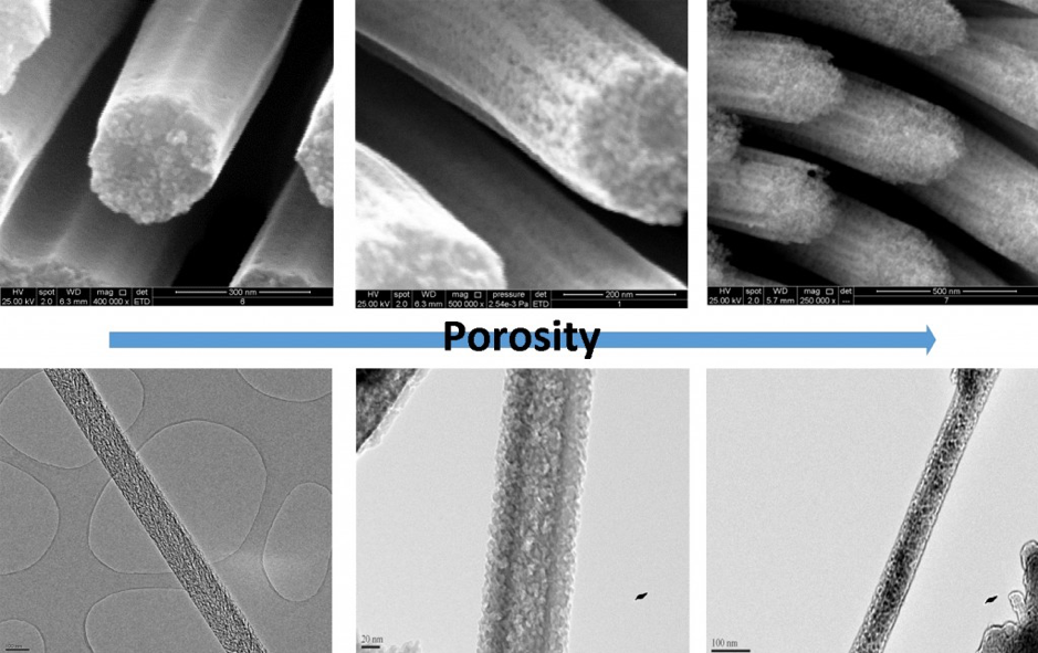
Silicon nanowires can also be produced from silicon wafers. In our laboratory, these nanowires are produced through a metal-assisted chemical etching (MACE) process that does not require a current to be applied through the silicon wafer. In this process, a silver metal template on top of the silicon wafer acts as a catalyst site for anisotropic etching with hydrofluoric acid. By patterning ordered circular arrays into the silver template, freestanding silicon nanowires can be produced with different diameters and heights. By varying the etching solution, these nanowires can also be made porous, dramatically increasing their surface area. Post-processing again allows these porous nanowires to be removed from the bulk silicon substrate, to be obtained as individual particles.
Silicon nanowires and porous nanowires are currently being investigated for cell transfection/therapy, drug delivery and chemical sensing applications.

Surface engineering of silicon nanomaterials
Surface engineering of silicon nanomaterials. Many surfaces and materials require chemical modification to suit a desired application. As such we have a range of surface modification techniques at our disposal.
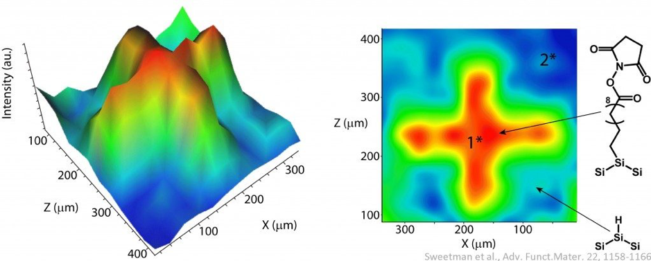
Hydrosilylation chemistry is used to react Si-H species with alkene or alkyne compounds. These reactions are usually thermally or UV-light driven and result in the formation of a stable Si-C bond. Hydrosilylation reactions are commonly performed on freshly etched porous silicon surfaces to generate a stable organic monolayer and incorporate desired pendant chemical functionality including carboxylic acids, esters and polyethylene glycol.

Thermal and ozone oxidation techniques are used to generate a thin oxide layer on surfaces. These surfaces can be subsequently used for silanisation reactions, where alkoxy or chloro silanes can react with surface –OH species via a condensation reaction. This allows the surface to be modified with specific, terminal chemical functionality, including amines, thiols and isocyanates.
Other surface modifications techniques, such as thermal hydrocarbonization and thermal carbonization are also employed for porous silicon functionalisation. All of the mentioned modification techniques are generally used to stabilise the surfaces and to introduce specific chemical functionality, be it reactive groups for conjugation of other species or low-fouling functionality to prevent protein and biomaterial adsorption.
Surface engineering by polymer grafting (to and from) is also used to generate functional surfaces for applications in cell culture, drug delivery and biosensing. Polymerisation techniques such as ATRP, RAFT and free radical are all used, depending on the specific application in mind.
As well as modifying surfaces through polymer grafting, plasma polymerisation is also used to introduce specific functionality to materials. Plasma polymerisation allows thin polymer films to be deposited onto a surface and can be used to generate a wide range of different polymer coatings with different chemical functionalities. This technique can be applied to most substrates, making it a highly versatile surface engineering method.


